
Advanced Packaging/Outsourced Assembly and Test (OSAT)
Packaging has significantly increased in importance for AI since it is a key enabler for increased I/O bandwidth. OSAT players stand to benefit as TSMC remains hesitant to expand packaging capacity

Investment summary
ASE Technology
19x 2026 PE
Leading OSAT globally with key operations in Taiwan
Strategic advantage of being located near TSMC leading edge fabs
Likely receiving majority (est >70%) of outsourced CoWoS work (i.e. WoS portion) from TSMC
Currently most CoWoS is fully packaged by TSMC end to end
However they likely outsource 10-15% of the WoS portion to OSAT like ASE
This outsourcing likely to increase as CoWoS demand increases
Also has own CoWoS-like technology with FOCoS (CoWoS-R like) and FOCoS bridge (CoWoS-L like)
Unconfirmed which customers are planning for adoption
Management noted multiple ASIC customers
With revenue contribution in 2026
Rumored to also be doing the packaging for NVDA Vera CPU and AMD Venice EPYC server
Also investing in testing to go along with packaging
Is higher gross margin (mid 30%s) than corporate average
Leading edge advanced packaging (including testing) contributes ~12% of ATM (assembly, test, materials) business or 8% of total revenue (2025)
Amkor
28x 2026 P/E
Key swing factor is Amkor’s $7b investment in Arizona, US
To go alongside TSMC fabs
Will be packaging Nvidia GPU as well as Apple M series initially
This likely is at the expense of ASE who currently is TSMC key partner in Taiwan
However, phase 1 (~$2b) is expected to be completed mid 2027, with production commencing early 2028
With phase 2 subject to customer demand
Currently single digit % of revenue attributable to AI
Rumored to be doing the packaging for Broadcom Tomahawk 6 switches and Nvidia GB10 for DGX Spark
TSMC
20x 2026 P/E
Gaining share in packaging driven by ‘Foundry 2.0’ company strategy
Synergies between foundry and packaging for higher yields
TSMC being conservative by offloading excess demand to OSAT players
Also outsourcing lower margin portions of CoWoS (i.e. oS)
However, may be too conservative, forcing ASIC customers to look elsewhere for advance packaging
Also as CoWoS-like packaging technology matures, should see increased competition from Intel IFS and other OSAT
Also shift to purely RDL interposer (no silicon interposer) should see share shift to OSAT
As well as shift to panel interposer in 2028+
King Yuan Electronics (KYEC)
26x 2026 P/E
Has most exposure to final packaged test for AI GPU
Likely does final package test for NVDA CoWoS sent from TSMC
ASE likely does the final package test for the CoWoS packages they do the WoS portion for (~10-15%)
Have increased capex to $37b (>100% of 2025 revenue)
Could see doubling of revenue in ~2 years
KYEC has the highest % revenue that is attributable to AI/HPC at 25% (2024)
Powertech Technology (PTI)
26x 2026 P/E
OSAT that specializes in memory packaging and test
Has strong relationship with Micron, SK Hynix and Kioxia/WD
Heavily investing in fan out panel level packaging for next phase of CoWoS innovation, i.e. CoPoS
Rubin Ultra (16 x HBM stacks + 4 reticle die stitching) would require much larger interposer than currently available
Scheduled to ramp late 2027/2028
Plans to increase capex to NT>$40b (US$13b) in 2026, up from NT$19b (US$0.6b) in 2025 for panel level packaging
A stock to keep in mind for 2026
Packaging overview
Semiconductor packaging refers to the final stage of semiconductor fabrication
Received finished dies on wafer from foundry
Packages chip into its final form ready to be soldered onto printed circuit board (PCB)
Commonly referred to as ‘back end’ process
‘Front end’ process refers to creating the transistor and metal layers on the wafer
‘Back end’ process includes everything done after that
There are multiple steps in the packaging process, e.g.
Dicing the chips from the wafer into singulated dies
Testing the chips for defects
Enclosing the chip in protective casing
Create electrical connections that the PCB can use (e.g. solder bumps)
Practical example
Customer produces dies on wafer at TSMC
The wafers go directly from TSMC foundry to ASE facility
The dies on wafer are tested using automatic test equipment (ATE) to identify ‘known good dies’ (KGD) (i.e. wafer sort test)
Then the dies are diced and singulated to individual dies using high precision saws/lasers
KGD are then packaged using the specified packaging method (e.g. flip chip, 2.5D, etc.)
Final packaged is then tested again using ATE (i.e. final package test)
May also include system level test and burn in test
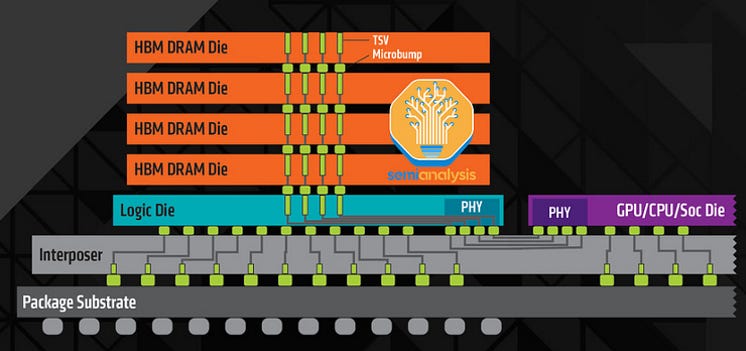
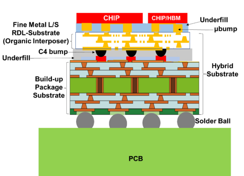
For heterogenous integration (combining multiple chips into a single package), it involves embedding the chips onto an interposer and/or substrate
Interposer is used to route interconnections between dies
Dies sit on top of the interposer
The interposer then sits on top of the substrate
Substrate is used to route electrical signals and power from the dies to the motherboard
The substrate then sits on top of the motherboard
Substrate connects to the motherboard via solder balls (i.e. ball grid arrays or BGA)
Outsourced semiconductor assembly and test (OSAT) refers vendors that do packaging and testing as a service
Historically, before the foundry/fabless model, packaging and testing was done inhouse by integrated device manufacturers (IDM) e.g. Intel, Samsung,
Types of packaging

Architecture
Contact Type
Wire
Contact Density
Substrate
Accuracy
Energy/Bit
5-101mm2
Organic/leadframe
20-10pm
1 OpJ/bit
Flip Chip
(1995)
Solder ball or copper
pillar
25-4001mm2
Organic/leadframe
10-5pm
O.5pJ/bit
TCB Bonding
(2012)
Heat compression force
Copper pillar
156-6251mlm2
Organic [Silicon
5-1 pm
0.1 pJ/bit
HD Fan Out
(2015)
1
Digita
RDL or copper pillar
500+1mm2
None
5-1 pm
O.5pJ/bit
Besi
Hybrid Bonding
(2018)
Hybrid bonding
Copper to copper
10K-1MM/mm2
None
0.5-0.1pm
<.05pJ/bit")
Wirebond
Chips are attached to a package substrate (or leadframe) and connected via fine wires (typically copper)
Relatively low cost and high volume
Generally used for >40nm process, for everyday electronics like TV, household appliances, etc.
Microcontrollers
Power devices
Analog integrated circuits
Many OSAT providers can do wirebonding
Compete on price, quality, track record, and low defective parts per million (DPPM)
Wirebonding process
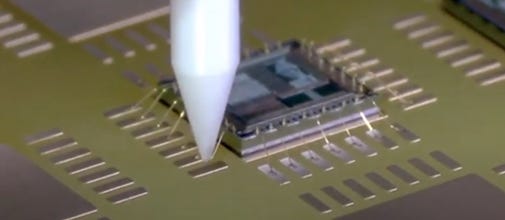
Process is done using a wirebonding machine
A bonding capillary (the pen like tool) has a tiny hole that feeds the wire through
The capillary pressures the wire onto the pad while applying force/heat/vibration
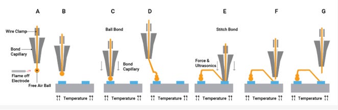
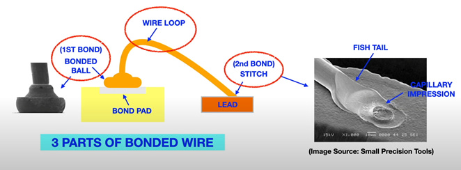
End of the wire from the capillary is heated to form a ball
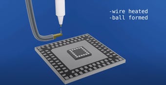
Capillary then presses the ball onto the die’s bond pad, while applying force, heat and ultrasonic energy (i.e. thermosonic bonding)
Then wire is spooled out and carried over to the package leadframe forming a wire loop
Again applying thermosonic bonding to connect to the leadframe pad
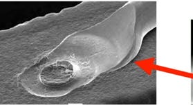
The wire is pressed against the pad using heat, force and ultrasonic energy. Then clamped off forming a wedge/stitch bond
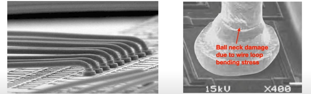
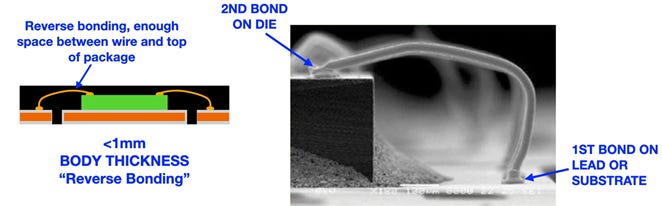
Low loop profile can be used for thinner package (<1mm)
This can be done by bending the wire forward and backwards using the capillary after the bond ha bee made on the die pad
However, there is limitation on how low the loop can be before damaging/breaking the wire
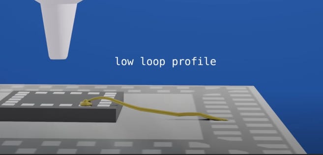
Alternatively, ‘reverse bonding’ can be done where the ball bond is first done on the substrate, and then on the die pad
Reduces stress on the ball neck
However, stitch bond cannot be directly done on the die pond bad
Because the capillary impact will damage the die surface
A bump must be first bonded on the die pad, and then the stich is bonded on top of the bump
Process is called ball (or bond) stich on ball or (BSOB) or stand off stitch bonding (SSB)
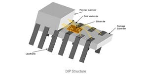
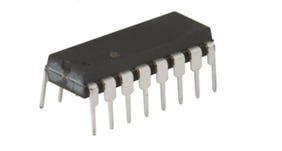
Dual in line package (DIP)
One of the earliest type of chip packages and is still widely used today
Use of leadframes which is a sheet of metal stamped to form leads
Have leads extending out from two opposite sites
The chip is attached to a die ‘paddle’ then wirebonded to the leads
Whole thing is then molded in plastic
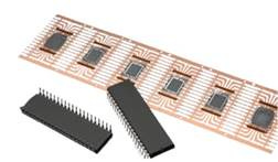
Note the leads are designed to go through holes in the PCB and then soldered onto the other side (‘through hole’)
Typically 8-64 pins/leads with 2.54mm pitch
Small outline package (SOP)
SOP is a package with ‘gull wing’ leads extending from two opposite sides
Typically 8-48 pins/leads with ≤1.27mm pitch
Note the leads are L-shaped and soldered directly onto pads on the PCB

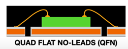
Quad flat no leads (QFN)
Unlike SOP, QFN has no leads
Instead connections are made via metal pads on the bottom of the package
Typically thinner profile than SOP
Because there are no leads, it minimizes space occupied on printed circuit board
Quad flat package (QFP)
Has leads extending from all four sides
Thus accommodating higher number of connections than SOP
Can be upwards of 300 pins/leads
Flip chip
Introduced in late 1990s/early 2000s
Also known as Controlled Collapse Chip Connection or C4
Wirebonding is limited to the edge of the die
Whereas flip chip can use the entire surface area of the die
The chip is mounted directly onto a substrate (or even circuit board)
Uses solder bumps instead of wires (used in wirebonding) called ball grid array (BGA)
Connections are in the form of array of solder balls on the bottom of the package
Instead of wires coming out only on the edge
Advantages relative to wirebonding
Shorter signal path (0.1mm v.s. up to 5mm for wires) which reduces inductance and resistance
Important for high speed/high frequency applications (e.g. 5G, AI/HPC, etc.)
Higher I/O density
E.g. can have >100,000 solder bumps per die
Connections can be made across the entire area of the chip as opposed to just the sides for wirebonding
Eliminates bulking wire loops allowing for thinner, smaller packages
Direct contact with the substrate allows heat to dissipate more efficiently
Also allows the back of the chip (where heat is generated) to be exposed and cooled
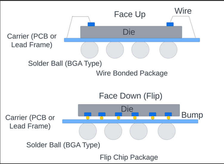
Flip chip process
Solder balls (bumps) are placed across the entire surface of the chip while it is still on wafer
Wafer is then diced into individual chips
Then start with substrate (typically organic laminate)
Include various layers for redistributing signals and power
Chip bumps then aligned to substrate pads and bonded via solder reflow
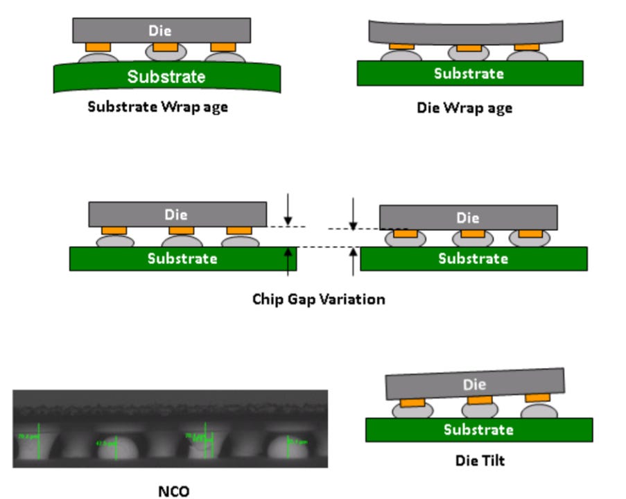
Some potential drawbacks of flip chip include
Warpage of either the substrate or die
Due to differing coefficient of thermal expansion (CTE) between different materials during reflow oven heating causing them to expand at different rates
Chip gaps caused by solder balls may making perfect contact with every copper pad
Die may not be perfectly flat
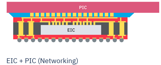
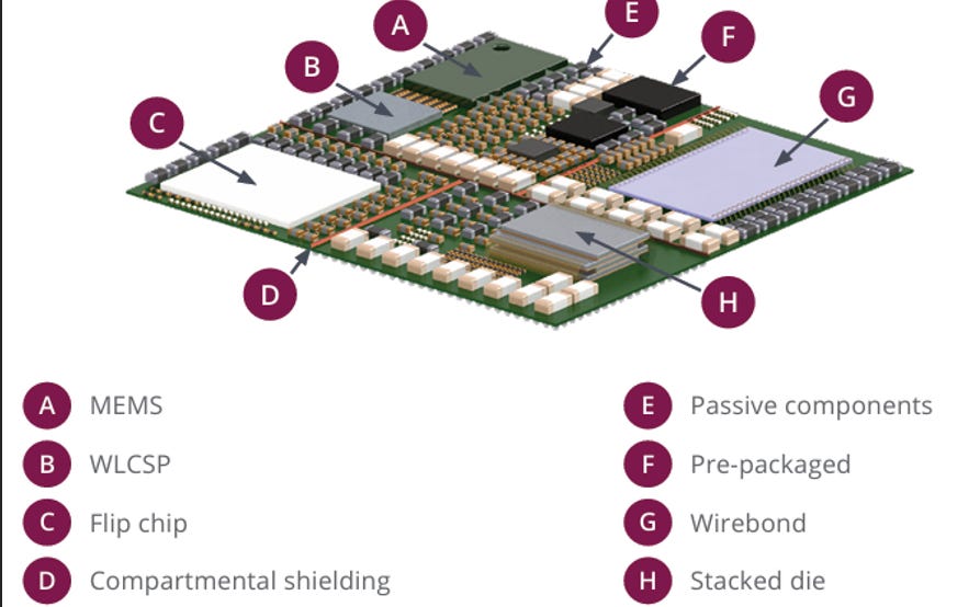
System in package (SiP)
System in package is a single package that contains 2 or more semiconductor dies
Rather than having separate chips on a large PCB
Effectively a ‘mini PCB’
May also include passive components such as resistors, capacitors, inductors, etc.
E.g. when transistors are turning on/off, there is a rapid change in current
Rapid change in current can cause a dip in voltage (like a momentary sag in pressure in a water pipe when you turn the tap on fast)
If the voltage drops too much, it can cause incorrect results (e.g. read ‘0’ instead of ‘1’)
A capacitor is a component that can store electrical charge
When the chip suddenly pulls current, the capacitor can quickly discharge that electrical charge (rather than pulling current from the power source)
This keeps the voltage stable
When things have calmed down, the capacitor recharges its electrical charge from the main power supply
This cycle happens millions of times per second, keeping the voltage clean and steady
In a SiP, the capacitor can be placed right next to the chip, sometimes even inside the package substrate or stacked on top
As opposed to on PCB where capacitors are further away
This provides faster response and more reliable performance
Other passive components used for
Prevent reflections and filter noise for RF and high speed signals
Reduce electromagnetic interference (EMI) using things like decoupling capacitors, ferrite beads or chokes, etc.
Tuning RF antenna
Supporting analog functions
Placing passives inside the SiP can save PCB footprint
Benefits
Save space by allowing shorter interconnections and higher density I/O
Also can integrate some components that would typically sit on PCB, e.g. DRAM, NAND, RF transceiver, etc.
Improved power/performance by shortening interconnections
Allow use of KGD instead of creating monolithic SoC
Common applications include
Connectivity module which includes transceiver for Bluetooth, WiFi, filtering, etc
RF front end modules which includes power amplifiers, switches, transceivers, filters, etc.
A variation of SiP is antenna in package (AiP)
Integration of antenna arrays on or in the package
E.g. for mmWave 5G modules
Manufacturing process
Wafer sort, grind and dice into singulated dies
Wafers are often thinned before dicing to maintain low package profile
Substrate (organic, ceramic or glass) is used which contains copper routing layers connected by TSV
Copper routing layers are used for signal and power delivery
Individual dies and passive components are placed onto the substrate
C4 bumps are created on the die
Dies are then aligned and bonded to the substrate pads
Then reflow and underfill
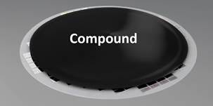
Epoxy mold then injected over the components and cured to form a hard plastic shell
Solder balls (BGA) are then attached to the bottom of the completed package
This allows it to be soldered onto the main circuit board
Substrate is then singulated into individual packages
SiP is often built in large panels for cost and scale efficiency
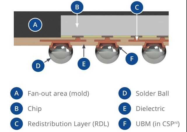
Fan out wafer level packaging
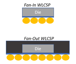
Fan out WLCSP allows the interconnections to be ‘fanned out’ beyond the surface of the die
Interconnections are made in a redistribution layer (RDL)
Solder balls are then placed on the top RDL layer, which connects to the PCB
Note there is no substrate layer
Wafer level chip scale packaging (WLCSP) means packaging the die while still on the wafer
Fan in WLCSP refers to a bumped die (i.e. effectively flip chip)
The package is the same size as the die
However the packaging is done while the die is still on wafer
RDL and solder balls are added directly on the wafer
As opposed to after the dies are singulated with flip chip
For fan in, the I/O is limited by the surface area of the chip
For fan out, the I/O can be expanded beyond the size of the die
Limited instead by silicon or organic interposer size
Can be very thin profile with high density interconnections
Commonly used for smartphone and wearables
Manufacturing process
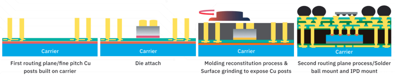
Singulated dies are placed onto a temporary carrier (glass or silicon)
Epoxy mold compound is applied and cured which encapsulates the dies
Then grind/polish to expose the die pads
Redistribution layers (RDL) are then formed layer by layer
Dielectric is first deposited
Lithography used to print lines and vias
Copper is then deposited into the lines and vias to form connection to the previous layer (or die pads)
Finally, solder balls are placed at the top layer
Which forms connection to the printed circuit board later
Individual packages are then singulated using saw/laser
Alternatively, the RDL layers can be fabricated first (i.e. chip last)
Then dies are placed onto the RDL
 bonding
Wafer molding
/ support wafer removal
RDL
Die
Chip-first method
Dice mounted on
metal-carrier
Wafer molding
/ carrier removal
RDL formation
Die
Resin
wafer
RDL
Singulation
Resin
wafer
External terminal formation
Singulation")
Panel level fan out (or panel level packaging or PLP) refers to the same process but just done on large rectangular panels
Fan out WLCSP is done on round wafers (300mm diameter)
But panels are much larger and rectangular (e.g. 600mm x 600mm) which is more suitable for packaging
Potential cost advantage compared to round wafers
However, more difficult to manage warpage and lithography uniformity
Examples include
TSMC integrated fan out (InFO)
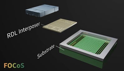
ASE FOCoS
Amkor SWIFT
2.5D packaging
Allows multiple dies to be packaged side by side on passive interposer
Interposer provides high density interconnect
~1/1um L/S compared to 15/15 – 5/5um L/S for fan out
Effectively a more advanced version of fan out package
Larger interposers than fan out
Can package different types of dies together (rather than just chiplets)
Interposer can be either silicon or organic
Can include integrated passive devices (IPD) such as capacitors, inductors, resistors, etc., embedded directly into the interposer
Helpful for AI/HPC devices that drive very high current and fast frequencies
Embedded decoupling capacitors help flatten impedance and mitigate voltage droop
For silicon interposer, it is typically fabricated on silicon wafer using 130nm or 65nm lithography to making traces and TSV
For organic interposer, RDL layers are fabricated on morganic material
Less costly as avoids silicon
Avoids deep TSV etch + copper electroplating process for silicon interposer
Organic interposer have much shallower vias
Silicon interposer made at foundry line with foundry pricing/margins
However, has larger L/S of 5/5 – 2/2um v.s. 1/1um for silicon interposer
Suitable for devices that have moderate bandwidth needs
Can also support larger formats
Beyond 3x reticle size which is the current limit for silicon interposer
However still needs to fit equipment which is made for 300mm wafer
In the future, there is shift towards panel level packaging which uses large 300mm x 300mm or 600mm x 600mm square panels
Can also have silicon bridge embedded in RDL interposer (i.e. local silicon interconnect or LSI)
Silicon bridge used for interconnections between die to die
I.e. provides ultra dense connections where needed
With rest of the routing handled by RDL
Currently used for Nvidia Blackwell GPUs
Although require to manage warpage issues due to different coefficient of thermal expansion (CTE) between organic interposer and silicon bridge
Can use low CTE substrate resin
Or add dummy copper to balance stress
Interposer is then connected onto substrate
This part is either done by the foundry (i.e. TSMC) or can also be outsourced to OSAT

Manufacturing process
Start with silicon wafer
TSV lithography patterned and etched
TSV used to connect the dies and the package substrate
TSV then filled with copper
Then RDL traces and vias are patterned and copper plated
Dielectric (SiO2) deposited using PECVD
Traces and vias patterned using lithography and etched
Then copper plated
Repeated for each RDL layer
Photoresist applied and patterned to form copper pillar patterns
Copper pillars then plated and capped with solder
KGD logic and HBM dies now attached to interposer using flip chip and reflow
Flux applied on interposer
Flip chip bonders then place the die onto the interposer pad
There is room for misalignment for bump-based bonding as solder has capillary forces which allow for self-alignment
Baked in reflow oven
Flux residue is removed
Gap between die and interpose then filled with epoxy resin
Wafer baked again to cure the underfill
Top dies then encapsulated with resin for mechanical support
CMP is used to smooth the surface
Package is now flipped and thinned by grinding and polishing
Until TSV on backside of interposer is revealed
Backside of interposer plated and bumped with C4 solder bumps
Package then diced into singulated package
Interposer now attached to package substrate using flip chip process
Entire package then encapsulated with protective layer

Substrate
Substrate provided by substrate providers
E.g. Unimicron, Ibiden, Nan Ya PCB, Kinsus, Ibiden, Shinko, AT&S, SEMCO, etc.
Substrate filled with copper wiring for routing
CoWoS typically uses Ajinomoto build up film (ABF) based organic substrate
ABF substrate typically made up of layer stack configured in X-Y-X where
X is the number of build up layers on the top and bottom
Build-up layers made from Ajinomoto Build-up Film (ABF) or similar material for fine line routing
Y is the number of core layers (often copper)
Provides mechanical support and power distribution
E.g. 5-2-5 substrate is made up of 5 buildup layers on top, 2 core layers, 5 bottom buildup layers
High end CPU packages may use 9-2-9 or 10-2-10 e.g. AMD EPYC, Intel Xeon, etc.
Can use less ‘build up’ layers if more of the routing is offloaded to the silicon interposer layer
Substrates are becoming larger with each CoWoS generation (i.e. CoWoS-S, CoWoS-R, CoWoS-R, etc.)
In the future, may start using glass substrates
Provides better stability at larger sizes
Also glass has better CTE matching with silicon
Expected timeline 2027
There is also developing of CoWoP (chip on wafer on PCB) which eliminates the need for substrates
This would be entirely done by OSAT houses
3D packaging
Taking an active die and packaging it on top of another active die
Typically will use hybrid bonding/TSV
Rather than C4 bumps or microbumps
3D packaging being used in
Sony CMOS image sensors
3D NAND stacking memory cell array and periphery circuit (e.g. YMTC Xtacking)
Backside power delivery networks
Copackaged optics
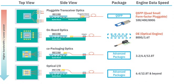
Silicon photonics offers data transmission with higher bandwidth and greater energy efficiency
Compared to conventional electronic integrated circuits which experience significant signal integrity challenges at high speed
Silicon photonics includes options from pluggables to integrated either on silicon interposer or substrate
Copackaged optics and optical I/O offer potential shortened electrical path to deliver even higher bandwidth
Mount photonics IC side by side with electrical die
Better efficiency (pJ/bit) and cost ($/Gbps) over pluggable optics
Copackaged optics est <5pJ/bit v.s. 20 pJ/bit for onboard optics and 30 pJ/bit for pluggable transceivers
One of the critical assembly steps in integrating the photonics IC is the optical fiber interface
Fiber arrays or optical connectors are aligned directly to the photonic chip coupling region
This could be edge‑coupling or vertical grating coupling, depending on design
Precision here is essential to minimize optical loss
Types of bonding
Wirebonding
Ultrasonic bonding
Uses combination of pressure and vibration between the bond wire and the bond pad
Produces cold weld between bond wire and pad
Used for aluminum wire to aluminum (or gold) pads
Thermocompression bonding (TCB)
Performed using combination of pressure and heat to form connection
Prevalent with gold wires for wirebonding
Bonding tools create ball bond at die site and wedge bond at the package pad site
But requires very high temperature of ~300-400 °C which can damage IC materials
Therefore not used prevalently today
Thermosonic bonding
Uses pressure, heat and vibration to make connection
Used when lower bonding temperature required (~180-250 °C)
Most common type of wirebonding today
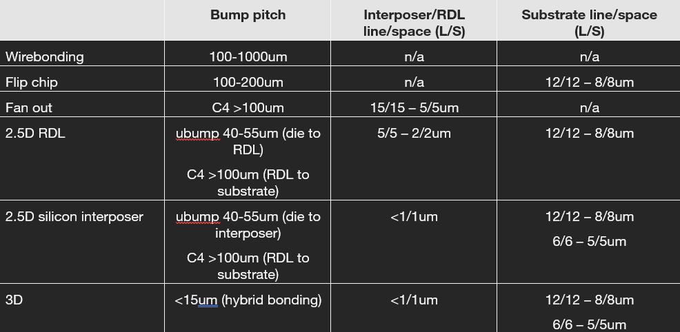
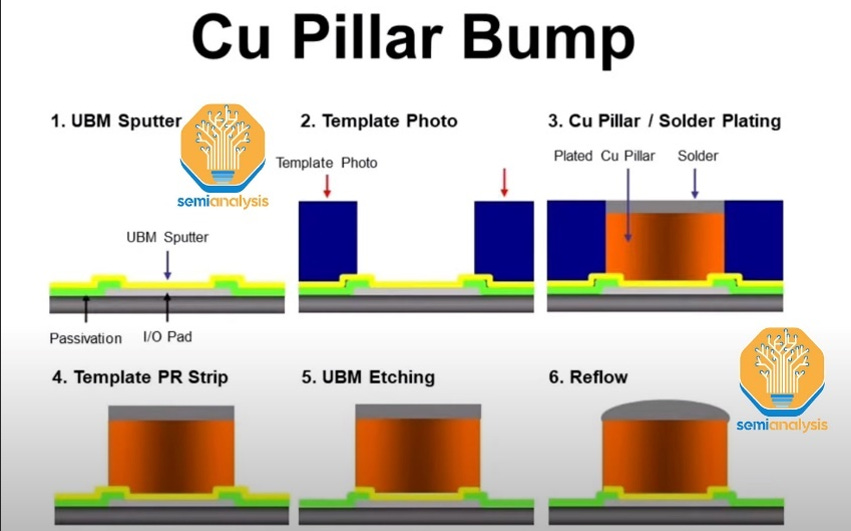
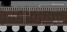
C4 bumps
Controlled collapse chip connection bumps (or C4 bumps) are relatively large solder bumps
Bump pitch 170-250 um
Bump height 70-100 um
Typically used to connect the chip to organic substrate using flip chip
Typically bonded via reflow soldering
A chemical agent (flux) is applied to the substrate copper pads to remove potential oxide layers present
Also reduces surface tension of the molten solder, ensuring it spreads evenly across the contact area
The stickiness of the flux also helps hold the chip in place before the reflow process
Die is then aligned so that the bumps match to the corresponding pads on the substrate
Done in batch process so many dies are placed all at once
Heat is applied to melt the solder bumps, forming a solid metallurgical and electrical bond (‘reflow’)
Done in reflow oven (or continuous reflow belt furnace)
Reflow refers to the process where the solder bumps are melted slightly and reform creating electrical connection
The remaining flux becomes resident that must be removed
Often flux is water soluble, so can be removed by water
Although some modern fluxes does not required to be cleaned afterwards
An insulating epoxy resin (underfill) is injected into the gap between the chip and substrate to provide mechanical strength

Microbumps

Fine pitch interconnects
40-130μm pitch
Max bump height of ~100um
Used typically between
Die to RDL
Die to interposer
HBM dies
Usually in the form of copper pillar bump structure
Better heat dissipation performance
Greater control of join diameter and stand off height compared with solder bump
Thermocompression bonding typically used here
Solder bumps are aligned to pads on the interposer/die/etc
Combination of pressure and heat (~200-300°C) is applied
Can also use rapid vibration which breaks up oxidation of metals on the copper bonding pads and solder balls
Thermocompression bonding used instead of solder reflow due to
Higher precision
Lower voiding
Better warpage control as avoids oven reflow process
Heat is applied from the top of the chip so only the chip and the microbump heats up
Minimizes substrate warpage
Compatible with temporary carrier wafers and fan out assembly flow
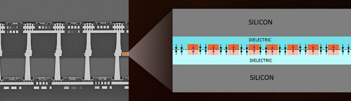
Hybrid bonding
Hybrid bonding allows to scale down to <10μm pitch
Approx 4-5x tighter pitch
Instead of solder, the interconnects are directly connected with copper pads (i.e. bumpless)
I.e. the top and bottom die are flush against each other
The copper pads are then connected to copper TSV which connects to the metal routing layers
Typically copper vias are patterned and electroplated within dielectric layer
Most commonly SiO2 or SiCN
Purpose of dielectric layer is to reduce interference between the vias
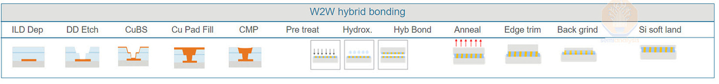
Can be completed either wafer to wafer (W2W) or die to wafer (D2W)
Wafer to wafer (W2W)
Two fabricated wafers are bonded directly together
Applications include CMOS image sensor, 3D NAND, BSPDN
Offers higher throughput
Only need to do alignment once per wafer v.s. once for every die on the wafer for D2W
However, not able to bin/test dies before the bond step
Thus typically used where the die yields are already high
A variation of W2W is ‘collective die on wafer’
The individual dies are KGD sorted and then temporarily bonded on reconstituted wafer
Then undergo W2W bonding
Copper vias and pads first formed
Wafer then aligned in chamber
Current W2W bonders can achieve alignment accuracy of <50nm
Then moved to heat chamber in vacuum where the wafers are pressed together with a small pressure for ~20 minutes to form the initial bond
Post bond inspection is done in situ via acoustics
If the alignment is insufficient, the bond can be reworked
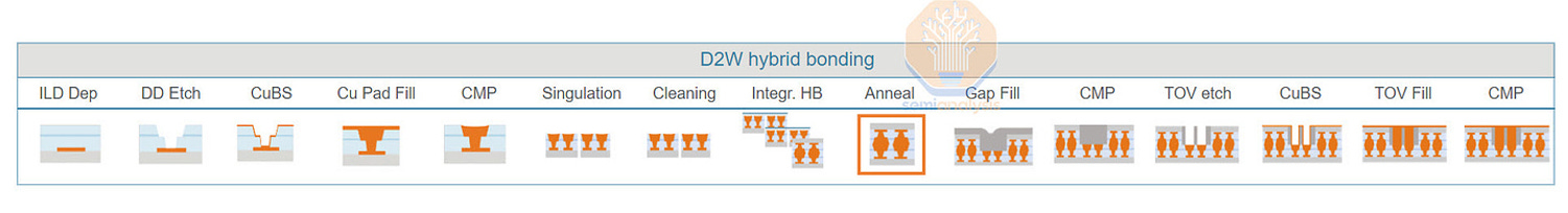
Die to wafer (D2W)
KGD are singulated from wafer and individually attached onto another wafer
Die pick and placed by bonding tool
‘Pick up’ however introduces contaminants and particles
Also slower to pick and place at approx ~1500-2000 dies per hour (Besi)
Although throughput slower in practice to ensure high alignment accuracy
However, can test KGD so not wasting silicon
D2W bonder equipment providers include Besi, ASMPT, Shibaura Mechatronics
Wafer sort test done on wafer to identify KGD
Note that probing can cause small damage on the copper pad surfaces
Require to be smoothed out for hybrid bonding

Dies are then diced and singulated
Laser dicing is preferred to blade dicing due to less particles/contaminants
Plasma dicing can also work but it is much lower throughput
The bottom wafer then sits on a wafer chuck
The dies to be bonded sit on a tape frame
Robotic arm then picks up the individual die
Typically there are 2 x robotic arms working in parallel to increase throughput
Die is then aligned using optics (camera) and set of alignment marks
For 3um TSV pitch, alignment needs to be ±0.5um
The robotic arm then places the die in the desired location and applies a bit of pressure
One of the most time consuming steps is to physically place the die on the wafer
This is because extra time is required for high accuracy alignment
Also extra time is needed to ensure any trapped air between the bond surface is propagated out
Benefits
Direct copper connections have much lower resistance and therefore lower power when sending electrical signals
Drawbacks
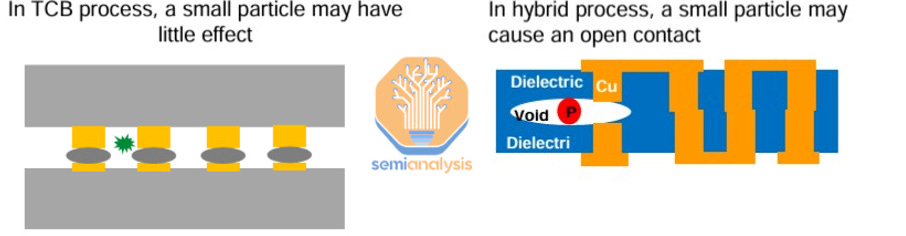
Very sensitive to particles which can lead to voids between the copper vias causing an open circuit
Require ISO 3 clean rooms
Common for foundries, but less common for OSAT players
Manufacturing process
TSV created in the silicon die through the transistor layer
Wafer coated with photoresist and patterned
TSV then etched using deep reactive ion etch (DRIE)
Barrier layer (e.g. titanium or tantalum) then deposited using CVD
Seed layer then deposited
Copper then filled using electrochemical deposition (ECD)
Chip is then flipped around and the backside of wafer is grinded until TSV is revealed
Copper pads are then formed using damascene process
Dielectric (SiO2 or SiCN) deposited
Holes for copper pads patterned over copper TSV and etched
Barrier and seed layer deposited, and then plated with copper
Chemical mechanical planarization (CMP) process used to grind down and smooth the dielectric surface
Bonding surfaces needs to be very smooth and planar
However, copper gets polished away fast than SiO2 dielectric by CMP
This means that the copper gets grinded down to a lower level than SiO2 i.e. over polishing (called ‘dishing’)
The exact profile of the dishing needs to be controlled
This can be mitigated by using a copper alloy instead of copper
Or use a proprietary CMP process with different slurries
The copper pads needs to either be recessed (>1um pitch) or protrude (<1um pitch) depending on the pitch of the copper pads
Typically recessed 5nm below the dielectric layer
This is to ensure that the copper does not get in the way of the dielectric to dielectric contact during annealing
Although if the copper is too recessed, then the copper to copper bond will not form

Two surfaces are now treated with plasma to ‘activate’ the surface
This enables the initial weak (Van Der Waals) dielectric to dielectric bond at 200°C in heat chamber
Then heat chamber is raised to 350-400°C for the copper to copper bond
The recessed copper expands at this temperature so that they contact
Thus the recession depth must be very accurate, as undergrowth will mean the proper bond is not formed
Testing overview
OSAT vendors purchase testing equipment such as
Automatic test equipment (ATE)
Wafer probe machines
Tokyo Electron is market leader
Ovens for burn in tests
Modules for system level test
OSAT vendors then charge a $ per hour for advanced devices, and $ per unit for high volume products
Testing typically commands higher gross margin due to lower capital intensity
Both KYEC and ASE testing have mid 30% gross margin
Compared to mid 20s% gross margin for packaging
Advanced packaging is higher gross margin
Testing gross margin is highly dependent on utilization
Average utilization is 65-70%
Testing can be categorized into phases such as wafer probe, final package test, etc.
Currently wafer probe is mostly done at Amkor and ASE
However, both are investing in final package test, including burn in and SLT
KYEC dominates in final package test
Industry themes
OSAT outsourcing gaining prominence
OSAT providers are taking larger share of the packaging and testing TAM due to
Fabless companies gaining share in their respective markets (e.g. AMD, NVDA, Apple, Qualcomm, etc.) over IDM
IDM increasing outsourcing (e.g. Intel, Samsung, Texas Instruments, etc.)
Fabless companies are purely design firms that outsource manufacturing to providers (e.g. foundry, OSAT, etc.)
Thus as fabless companies increase their share of sales in the market, the TAM for OSAT expands
IDMs are also increasing their outsourcing to OSAT
As devices get more complex, it requires increasing amount of R&D and capex resources to keep up with technological trends
OSAT have more scale to amortize fixed R&D spend over
OSAT can also maintain higher utilization on packaging equipment
Packaging equipment is quite fungible between packaging type and customers (Amkor, ASE)
Therefore, it is possible to better smooth out seasonality between different end markets (e.g. smartphone, PC, server/AI/HPC, auto, etc.)
And maintain high utilization of equipment
Cleanroom constraints
May need to ramp quickly for a new product
Inhousing packaging and testing would require expanding/building up new cleanroom space, ordering equipment (3-6 month lead time), etc.
OSAT provider can get packaging/testers up and running for a customer in weeks
IDM/foundries may have fabs in certain locations without the complementary packaging/test facility
Instead can outsource to OSAT in that region to avoid overseas shipment
IDM also tend to outsource low end packaging e.g. wirebond, etc.
Can reduce capital intensity by outsourcing packaging and test
To accommodate for increase capital intensity in front end manufacturing
Intel specifically may start increasing outsourcing since the operational split between design and foundry
IDM accounted for 35% of ASE revenue (3Q25)
For testing, outsourcing benefits include
Faster ramp
Potentially lower cost due to scale and higher utilization
Do not require to invest for peak demand
Although this would make OSAT revenue more cyclical to semiconductor swings
CoWoS
Customers will initially go to TSMC for turnkey service to guarantee yield and fast time to delivery
However as time goes on, more portions of packaging/testing can be outsourced as the technology matures
Regulatory control/tariffs
US Bureau of Industry and Security (BIS) created list of approved IC designers and approved OSAT companies
Certain high performance chips and ICs require BIS license to be exported/reexported/transferred outside US
However, there is an exemption if that chip is exported to OSAT company for packaging
List includes ASE Technology, Amkor, Powertech Technology, TSMC, UMC, Samsung, etc.
Generally does not include Chinese firms
Intention is to avoid sending advanced chips to China without a license
Where US export controls may be circumvented
E.g. if Nvidia Blackwell chips were to be packaged in China
ASE Technology has divested their China OSAT facility in response
US imposed sweeping tariffs to multiple countries globally on Apr 25
If OSAT packaged a chip and is shipped to US, tariffs may apply
Tariffs charged based on country of origin
This is generally where the imported product was ‘made’
I.e. where the last substantial transformation occurred
For chips, customs typically treat the packaged chip as originating in the country where the final assembly/packaging was done
Wafer made in Taiwan, packaged in Taiwan, sent to US
Will be classified as Taiwan origin. Standard duties will apply
Wafer made in Taiwan, packaged in China, sent to US
US customs likely treat as China origin
Because last substantial processing (packaging) was done in China
Semiconductors in China currently fall under Section 301 list, which is subject to 50% tariff
From 1 Jan 2025, the existing 25% duty on semiconductors from China doubled to 50%
Although tariff situation on Chinese semiconductors/electronics is in flux
Trump announced a new tariff to be imposed on Chinese semiconductors
But this additional tariff (in addition to the 50% existing tariff) is set to 0% initially, delaying any increase until Jun 2027
Wafer made in US, packaged in Taiwan, sent to US
Likely still treated as Taiwan origin, despite wafers made in US
Standard Taiwan duties will apply
Wafer made in US, packaged in Taiwan, sent to US
Likely still treated as China origin
Section 301 tariffs likely to apply
Wafers made in US, packaged in US
No import tariff apply at all
US CHIPS Act provides incentives for advanced packaging through direct funding grants
As part of the total $39b manufacturing incentive pool
Amkor has been awarded $407m in direct funding for their advanced packaging and test facility in Arizona (Dec 24)
Located close proximity to new TSMC wafer fab facility
Amkor has committed up to $7b total investment through multiple phases
Also eligible for the Advanced Manufacturing Investment Tax Credit scheme which is 35% for qualified investment in semiconductor manufacturing facilities including OSAT and advanced packaging
One Big Beautiful Bill Act increased tax credit from 25% to 35% (Jul 25)
Applies to depreciable tangible personal property related to manufacturing operations
Can be used to offset future tax obligations
US currently has ~3% of global advanced packaging capacity
Advanced packaging favors one stop shop vendors with both packaging and test facilities
Currently, individual GPU and HBM dies are individually tested. Then fully packaged together and tested again
This is the ‘final package’ test that is currently being outsourced to OSAT
However, there is talk of testing the package in various intermediate steps, e.g.
Testing silicon or RDL interposer (i.e. known good interposer)
Testing GPU on interposer
Then testing HBM on interposer
If testing is done in between packaging steps, then it makes more sense for both packaging and testing to be in one place
I.e. good for OSAT vendors that provide both packaging and testing (Amkor, ASE, PTI)
May be bad for pure play testing players like KYEC
Currently ~44% of KYEC revenue is in final package test (2024)
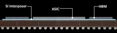
TSMC CoWoS
Currently majority of AI accelerators (+HBM) are packaged on TSMC CoWoS
TSMC monthly CoWoS capacity is estimated to be around 75-80k wspm (900-960k wafers annually)
It is rumored to increase to 120-130k wspm (1.4-1.6m) by end of 2026 ( https://www.trendforce.com/news/2025/12/08/news-tsmcs-cowos-l-s-reportedly-fully-booked-osat-partners-step-up-with-ases-cowop-in-focus/?utm_source=chatgpt.com)
“According to Commercial Times, TSMC’s AP8 facility in Southern Taiwan Science Park and AP7 in Chiayi have begun equipment move-in this quarter” (Dec 25)
NVDA currently dominates CoWoS capacity
ASE and Amkor are both certified OSAT providers
Scheduled for completion in mid 2027
Likely packaging technology used for each generation
Ampere (A100): CoWoS-S
Hopper (H100/H200): CoWoS-S
Blackwell (B200/B300): CoWoS-L
Rubin: CoWoS-L
Rubin Ultra: CoPoS (likely)
Rubin CPX: fan out (potentially)
Other CoWoS demand includes
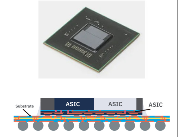
AMD for MI series and Xlinix products
Broadcom for Google TPU, and also new Tomahawk switches (JPM)
ASICs from Meta, OpenAI, AWS
TSMC by default does the full flow CoWoS process including CoW and WoS portions
However, TSMC has outsourced some of the wafer on substrate (WoS) work to OSAT vendors
I.e. form C4 bumps on interposer to connect with substrate, reflow, underfill, encapsulate, then form solder balls on substrate for PCB mounting
ASE is believed to dominate the outsourced WoS work in Taiwan
Amkor is mainly targeting the US ramp in Arizona
This likely is to increase over time as demand continues to increase
TSMC rumored to have completely outsourced WoS portion for CoWoS-L (JPM)
TSMC is also outsourcing final package test to OSAT vendors such as ASE and KYEC
Currently TSMC likely does the wafer sort test (for known good GPU die), as they will need to do the CoW portion before sending to OSAT
ASE likely does final packaged test for the ~10-15% of CoWoS wafers which they do outsourced WoS for
KYEC likely does the other (majority) share for final packaged test
TSMC likely send the full CoWoS package to KYEC (rather than just CoW)
Rumored that TSMC will begin outsourcing the full CoWoS flow to OSAT beginning late 2026
TSMC motivated to outsource because
WoS portion is standard flip chip which has lower margin (below corporate average of high 50s%)
May start outsourcing CoWoS-S in preparation for more complex CoWoS-L
Also with panel level packaging set for mass production late 2027, there is risk of overcapacity for TSMC in wafer packaging
I.e. CoPoS (chip on panel on substrate)
However there are challenges with ‘through glass vias’ and mechanical stability
TAM
Total OSAT market is approx $40-50b annually
Includes both packaging and testing
Market is expected to grow low teens %
Driven by broader semiconductor market
Typically packaging/testing intensity as % of semiconductor capex remains relatively flat as single digit %
Although that may be increasing for advanced packaging and testing
Packaging typically is 75% of market v.s. testing at 25%
Packaging range from 15-25% gross margin, whereas testing can be 25-35% margin
Packaging tends to be more capital intensive, whereas testing is more IP intensive
Range is due to logic/IC (higher margin) v.s. memory (lower margin)
TAM is impacted by the share of outsourced v.s. inhouse
The outsourcing share continues to increase for the reasons aforementioned
Logic IDM limited to Intel and analog players
There is higher rate of inhousing from memory players e.g. Samsung, SK Hynix and Micron
Competitive landscape
ASE Technology is dominant player in Asia supply chains
Including Taiwan for advanced nodes
Amkor is leader in automotive. Also key OSAT provider to Apple
KYEC has been significantly ramping test capability for AI/HPC
TSMC, Intel and Samsung all have advanced packaging capabilities which they offer to external customers
Effectively reduces TAM of OSAT providers
However, all 3 partners with OSAT providers to expand capacity and outsources certain parts of it
OSAT providers help foundry/IDM ramp advanced packaging capacity faster
OSAT also have facilities globally that the foundry/IDM may not be present
Can outsource lower margin parts e.g. ‘wafer on substrate’
Packaging equipment is relatively fungible, so OSAT can achieve higher utilization on equipment
Allowing to provide advanced packaging cheaper
Whereas if TSMC overbuilds on CoWoS capacity, it less options available to change the capacity for something else
Also foundry/IDM may have more expertise in wafer + silicon interposer fabrication
But less expertise on organic interposer, substrate design, thermal considerations, assembly flow, testing, cost optimization, etc.
When choosing OSAT provider, the key considerations include
Scale
Whether the OSAT has enough scale to handle large volume devices
Capacity availability
Whether the OSAT can ramp up capacity when needed, e.g. AI/HPC
Packaging yield
Different OSAT providers will have different packaging yield
OSAT often provides a contractually ‘guaranteed’ yield
If yield falls below the guarantee, then the OSAT may provide damages
If yield is above the guarantee, then the OSAT may be provided a performance bonus
Packaging yield typically ranges between 90-95%
Packaging yield is becoming especially important for devices such as AI accelerators
The cost of scrapping a package is very high with GPU + 6-8 HBM stacks (each with 8+ DRAM dies)
Geographical location
Ideally the OSAT provider is located close to where the wafer is made
As the wafers need to be transferred from the foundry to OSAT provider
Customers prefer OSAT in close proximity to them
Customers often co design their devices with OSAT providers
Often pushing packaging technology to bleeding edge of what’s possible
Today, export regulatory controls and tariffs are also a consideration
Price
Typically priced on a per unit basis for packaging
For testing, it is based on cost per test hour basis
Pricing depends on
Design
Attachment rate
Long term loyalty
Trust
Technology
Overall solution
Sometimes customers may procure materials themselves, e.g. expensive substrate materials
Common to see price erosion clauses
e.g. 3-5% price reduction per year from expected efficiency gains
Some customers sign long term agreements to reserve capacity
Especially for capacity that requires new equipment investment
Substrate is provided by substrate providers
Ibiden (TSE 4062) provides substrate for NVDA
Other substrate providers include Shinko, Nanya PCB, Unimicron, and Kinsus
Substrate including insulating film supplied by Ajinomoto (TSE 2802)
China competition
There is increased competition for packaging in China
However, more so for mature nodes >7nm
However, China OSAT have begun investing for advanced packaging
Global OSAT vendors have also sold their China operations due to US BIS rules aforementioned
Non Chinese customers shifting OSAT needs outside of China (mostly to Taiwan)
Meanwhile, Chinese customers are sourcing locally
The net effect so far has been positive for non Chinese OSAT players
China is providing subsidies to build out its own packaging and test industry
Aligned with “Made in China 2025” initiative
Main China OSAT players include
JCET
Approx $5b revenue
Acquired STATS ChipPAC (2015) for flip chip capability
Include wirebond, flip chi, fan out, 2.5Dcapability
Tongfu Microelectronics
Approx $3b revenue
Has JV partnership with AMD in Suzhou and Penang plants
HT Tech (Huatian)
Approx $2b revenue
Affiliate with Hua Hong
Investing aggressively in high end packaging for AI
Also auto and memory
ASE Technology
Acquired Siliconware Precision Industries (SPIL) in 2018
Announced in 2016, but had to deal with regulatory hurdles
SPIL was #3 largest OSAT firm globally
ASE runs SPIL as independent company with its own customers and culture
Also acquired Universal Scientific Industrial (USI)
USI is a global Electronics Manufacturing Services (EMS) / Original Design Manufacturer (ODM)
Similar to Foxconn, Wistron, etc.
Does everything except for the final product assembly (e.g. assembling iPhone)
Does the final module assembly, taking the final packaged chip and producing a finished electronic module
E.g. takes the packaged chip and solders onto PCB
Also combines multiple PCB, modules, antennas, etc. into a self contained functional module
Has natural synergies with ASE/SPIL which does the chip packaging
Customers thus have one stop shop from wafer to final product (i.e. full turnkey service)
From packaging the chips
Testing the chips
Mounting the package on a PCB with other components
Testing the final product
Assembling the final product
Can reduce handoff and transit delays
Attractive for smaller IC design companies that want to minimize
Examples of electronic devices and module include
Smartphone, wearables and PC motherboards
Wireless connectivity modules (e.g. WiFi, bluetooth)
Display modules (e.g. flat panel display)
Power control modules
USI has been major backend SiP provider for Apple including
WiFi/bluetooth
Fingerprint sensor packages
Force touch controller modules
Apple Watch S Series SiP module
ASE Technology’s competitive advantages include
Scale
Largest OSAT provider in the world with ~1/3 market share
Able to provide customers with more assurance on capacity availability
Can handle large volume products (e.g. smartphones, wearables, IoT, auto, etc.)
Speed
ASE has historically demonstrated its ability to ramp up capacity to large volumes when needed
Is currently doing so now, with ~$3.5b equipment capex investment expected for 2025, almost double from $1.9b (2024)
Geography
Close to Taiwan supply chain
Taiwan is still where most of TSMC wafers are coming out from
Especially advanced ≤7nm nodes used for advanced packaging
ASE wants to continue expanding capacity in Taiwan
Following where the advanced wafers are being produced (i.e. TSMC foundry)
Believes that advanced packaging needs are rapidly evolving
Require R&D and operations to be in close proximity
Yields need to be constantly maintained generation by generation
Need to constantly tweak and change the configuration of packaging equipment
Believes it would be ineffective to do so from a satellite facility
Manufacturing
Have been investing in ‘lights out’ factories, i.e. fully automated lines
Can provide higher level of reliability and capacity
Approx 20% of capacity is fully automated (2023)
The entire factory process is also digitized
Capture data from every step of the process
Can share data with customers for transparency
Facilities and machinery capex has been increasing in intensity (as % of revenue)
Previously, facilities/machinery were generic and there was more commonality across factories
However, advanced packaging requires more specialized machine and equipment
Also with automation, the capex intensity is higher
Taiwan
Strategically located close to TSMC leading edge fabs
US
Currently no plans to build facility in US
Have been invited by customer to invest factory in US
Likely Apple and Nvidia
However, the economics is the main gating factor
Even with subsidies, the economics/return does not make sense
OSAT margins are quite slim, so less room to bear cost increases
However, SPIL (merged with ASE), was one of the announced partners to Nvidia $500b investment in manufacturing in US (Apr 25)
Mexico
Acquired some land in 2024
Will be able to service US
Malaysia, Korea, Singapore, Vietnam, Philippines
China
Disposed of China sites by the end of 2021
Due to regulatory export controls
Customers started to avoid packaging chips in China due to US BIS rules
4 plants located in Kunshan, Suzhou, Weihai, Shanghai
Primarily did traditional packaging
Sold to Wise Capital Road for US$1.46b
Go to market
Emphasize long term relationships with customers
Often co develop packaging innovation with customers (i.e. design for manufacturability)
Align packaging with customer roadmaps
Was first to launch 2.5D with AMD with Fiji GPU (launched 2015)
Had been working on 2.5D with AMD since 2007
E.g. if a fabless company is designing a new AI ASIC, ASE’s engineers might advise on bump layout or thermal solutions that align with ASE’s packaging capabilities
Will also co invest with customer
Customer may sometimes partially pay for new equipment
Or provide prepayment in exchange for reserve capacity
Promote engineering capability to industry via industry forums, e.g. SEMICON
Packaging
CEO has been very vocal about investment in silicon photonics packaging
Have been making investment in leading edge advanced packaging (LEAP)
Refers to ≤3nm node technology
Includes both advanced packaging (~80%) and testing (~20%) revenue
Includes FOCoS and FOCoS bridge revenue (3Q25)
~US$600m revenue in 2024, increasing to ~US$1.6b in 2025
Expected to increase >US $1b again in 2026
I’m estimating US$1.4b increase to $3.0b revenue in 2026
Contributing 11pcp of revenue growth and attributing 21% of packaging and test (‘ATM’) revenue
Note all the LEAP revenue is margin accretive
Test is ~35% gross margin (4Q24)
TSMS CoWoS outsourcing
Primarily does ‘wafer on substrate’ (WoS) portion of CoWoS
TSMC has stated that they don’t object ASE doing more of the CoWoS process
However gating factor is ramp up quality and reaching acceptable yield
ASE said it has TSMC support to guide them
Currently they are making investment for the CoW portion (2Q24)
Have engaged with multiple customers on FOCoS
Mostly from ASIC customers
Multiple customers have gained confidence on the technology over years of product development, trial and error, process materials, with different equipment, and reliability (2Q24)
Will start to see meaningful revenue come in 2026 (3Q25)
Will also be margin accretive
[Rumored AMD using ASE for Venice and other HPC products from late 2026 (JPM)]
[Also Nvidia Vera CPU]
Nvidia reportedly rumored to be working on packaging technology called CoWoP (chip on wafer on PCB) with SPIL
Eliminates the (expensive) substrate
Collaborate with Siemens Digital Industries Software OSAT Alliance Program to offer fully validated assembly design kit (ADK)
Adoption Siemens Xpedition Substrate Integrator and Calibre 3DSTACK technologies
Can significantly reduce FOCoS package planning and verification cycle times by about 30-50% in each design iteration
ASE offers the “VI Pack” which includes 6 advanced packaging solutions below
FoPOP
FOCoS
FOCoS bridge
FoSiP
2.5D/3D
Copackaged optics
FOPoP (fan out package on package)
Combines fan out bottom package with a standard package mounted on the top
Benefits
Thinner profile and better electrical and thermal performance compared to conventional interposer based package on package
The bottom package eliminates the need for interposer
Almost 40% reduction in height over substrate based package on package
Higher interconnection density
Shorter interconnect length
The development cycle time and cost can also be reduced since top and bottom packages can be decoupled from each other
I.e. qualification, yield, sourcing, procurement timing and logistic handling
Allows for increased complexity due to RDL on both sides of the die
Used for
Mobile applications that require high density interconnections and thinner package form factor
Pluggable optical transceivers and copackaged optics because of higher bandwidth
Much shorter interconnection between the photonic integrated circuit and controller
Improves energy efficiencies from 25pJ/bit to 5pJ/bit
Note, a semi additive process is used to grow the copper post and RDL copper routing
Used instead of traditional subtractive process where you deposit a layer of material and etch away what you don’t want
Traditional damascene process is too costly for backend packaging
Start with temporary carrier (glass or silicon)
Then deposit ‘release layer’ (for debonding step later)
Deposit polymer dielectric like polyimide or benzocyclobutene (PBO) as RDL base layer
Thin copper seed layer is then deposited
Required for copper electroplating step later
Thick photoresist is applied. Lithography used to pattern traces in RDL layer
Copper electroplating used to deposit metal routing
Then remove photoresist and seed layer
Step repeated for desired number of RDL layers
Deposit seed layer and much thicker photoresist for copper vertical post
Pattern openings where post should be
Copper electroplating used to deposit copper post
Remove photoresist and seed layer
First die is then aligned and attached to RDL traces using flip chip process
Entire structure is then encapsulated with epoxy mold compound (EMC)
Backgrinding process used to remove the mold compound from the top to expose the vertical copper posts
Second RDL stack is now built on top of the structure
Temporary carrier (glass or silicon) is then removed from the structure by chemically dissolving or debonding from the ‘release layer’
Package is flipped, and grinded to reveal copper posts
Second die now attached
Then entire package is singulated and tested
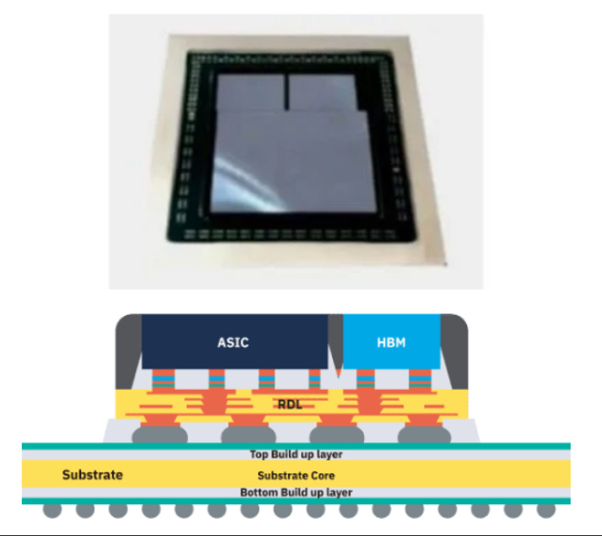
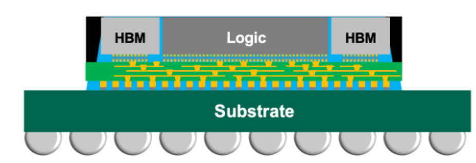
FOCoS (fan out chip on substrate)
Have been in production since mid 2010s
Chips are integrated onto fan out RDL, which is then attached to substrate
Similar to TSMC CoWoS-R
No silicon interposer which reduces package cost
Less warpage compared to silicon
Due to differing coefficient of thermal expansion between silicon and organic substrate
Also ASE offers reinforcement rings to reduce warpage
Mechanical stiffeners (typically copper or stainless steel) that surround or partially encircle the outer edge of a large fan out package
Can pattern L/S (line/space) of 2/2um for RDL interconnect
I.e. line (copper trace) width of 2um and gap between adjacent traces of 2um
High I/O counts (>1,000)
RDL ~3um thick
FOCoS chip first used when integrating smaller number of chiplets
Fan out size typically under 1 reticle size with ~2-3 RDL layers
Shorter die to die interconnects due to avoiding microbumps
Dies are connect with direct copper vias through RDL
FOCoS chip last used when integrating multiple chips (e.g. ASIC + HBM stacks)
Support larger interposer (>1 reticle size) and potentially more RDL layers for very high I/O and bandwidth
FOCoS chip first
2 (or more) KGD chips attached onto carrier wafer
Entire structure is then encapsulated with epoxy mold compound (EMC)
Then mold grinded and planarized to expose chip
RDL layers then formed
Dielectric deposited onto mold surface
Seed layer deposited
Photoresist deposited and patterned for traces
Copper electroplating used to deposit copper
Remove photoresist and seed layer
Repeat for multiple RDL layers
Vias then patterned through dielectric and plated with copper to form connection
Form bumps on RDL layer that will connect to BGA subtrate
Package is then singulated and flip chipped onto BGA substrate
Underfill and overmold used to provide mechanical reliability
FOCoS chip last
Start with temporary carrier
RDL layers then built on the carrier
Microbumps (or copper pillars) are created on the die first
Microbump is ~125x smaller than C4 bump, and ~8000x smaller than solder ball
Then chip is mounted onto the RDL pads
Followed by thermocompression bonding
Mold compound is then used to create mechanical support
Solder bumps then mounted onto RDL to be attached to BGA substrate
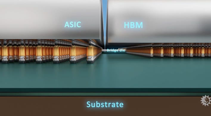
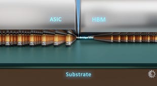
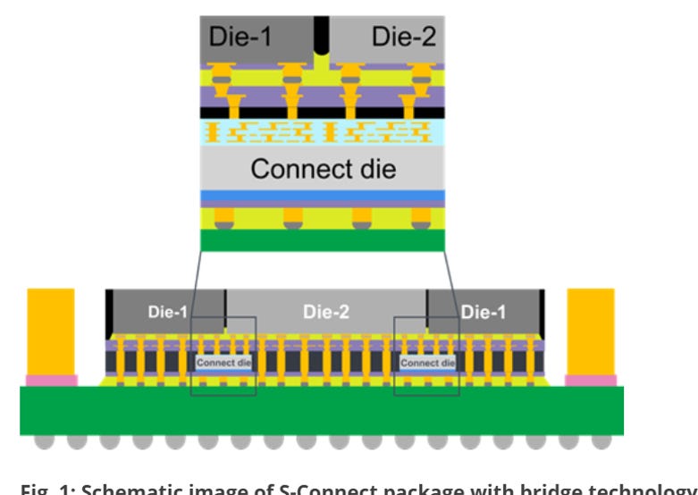
FOCoS bridge
Introduced 2023
Similar to FOCoS, but uses small silicon pieces with routing layers as ‘in package’ interconnects between chiplets e.g. between GPU and HBM
Provides similar electrical, signal, and power integrity performance to silicon interposer solutions
But at lower cost and without reticle size constraint
<1um L/S with die edge density of ~1000 wires per mm (of die edge) per layer
Compared to FOCoS of ~2um L/S with die edge density of ~500 wires/mm/layer
High I/O counts
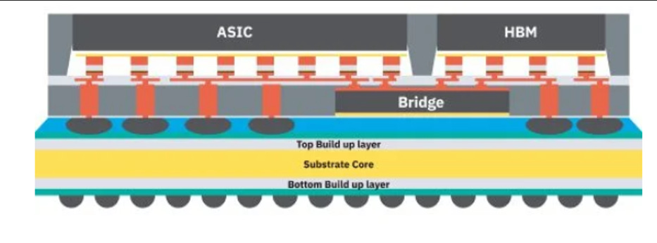
However requires ArF or immersion DUV for silicon die bridge fabrication
Suitable for high speed signal transmission required for AI/HPC devices
Targeting AMD or ASIC AI accelerators
Silicon bridges provide ultra fine pitch interconnection in packages
Can address the memory bandwidth bottleneck challenges in systems
However, it only uses silicon pieces in the specific areas where the chiplets are being connected
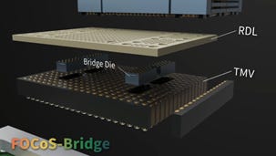
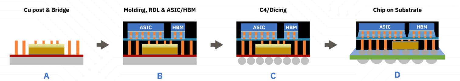
Start with carrier wafer
Silicon bridge die is attached to carrier wafer using microbumps
Vertical copper posts then plated onto carrier wafer around the silicon bridge
Fabricated using semi additive process over patterned photoresist
Diameter 70um, pitch 150um, height, 80um
Epoxy mold compound (EMC) is then used to encapsulate the die and copper posts
Then grinded expose copper posts and microbumps of the bridge die
Dielectric then deposited
Through mold vias (TMV) etched down through the dielectric to reach the copper posts and bridge die microbumps
FOCoS bridge with TSV introduced in late 2025 which adds TSV in the bridge die to provide vertical delivery path
Reduce resistance by 72% and inductance by 50% v.s. standard FOCoS bridge
RDL layers are then formed
ASIC and HBM dies are then attached
Followed by underfill and molding
Carrier wafer is then removed
Then C4 bumps are attached on the now exposed bottom side
These connect to the original copper posts
Fan out wafer is then diced and singulated into individual packages
FOSiP (fan out system in package)
Next evolution beyond standard SiP
Dies are attached onto RDL instead of traditional substrate
Difference is that the interconnections are fanned out in RDL layer
As opposed to regular flip chip attachment for SiP
L/S typically 2/2um compared to regular SiP of ~10/10um
FOSiP can be thinner than regular SiP
Interconnections in RDL can have higher density, so requiring less layers than traditional substrate (about 3 layers reduction)
Also more cost effective as it utilizes wafer level packaging
Compared to placing components on individual substrates with standard SiP
Up to 60,000 units per hour
Use cases include wireless modules, IoT, Bluetooth/WiFi, and RF front-ends where high mix and high volume are required
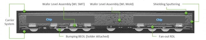
Manufacturing process
Start with carrier wafer
RDL is fabricated first (i.e. chip last approach)
L/S of ≤2um
Built using semi additive process
Microbumps then deposited for chip to RDL interconnection
Also solder bumps added on backside of RDL for attachment to substrate
Chips and passive components attached onto RDL layer
Entire package is encapsulated using molded underfill (MUF)
Underfill and encapsulation are done simultaneously using mold compound
The mold compound fills the under-die gap during compression molding
As opposed to underfill being a separate epoxy step after die placement
Thin metal coating may be applied over mold cap for shielding sputtering
Provides EMI shielding for RF modules
2.5D/3D IC
ASE also offers 2.5D packaging with silicon interposer on substrate
Similar to CoWoS-S
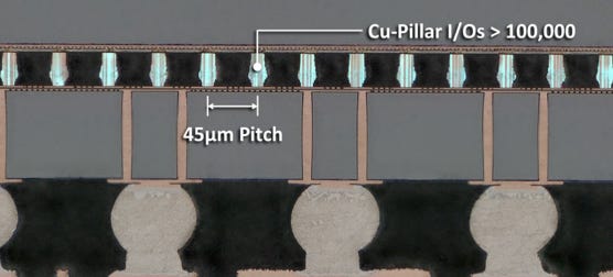
Silicon interposer is approx 100um thick
Ultra high density routing with L/S of 0.4/0.4um
Typically fabricated using 90nm/65nm
[Potentially outsource from UMC]
>100,000 copper pillar I/O with ~45um pitch
>400 microbumps/mm2
Interposer capable of embedding decoupling capacitor or active devices
Used for
High end GPU
High end FPGA
Network switch / router for data center & 5G infrastructure
AI accelerator for AI training/inference
Copackaged optics
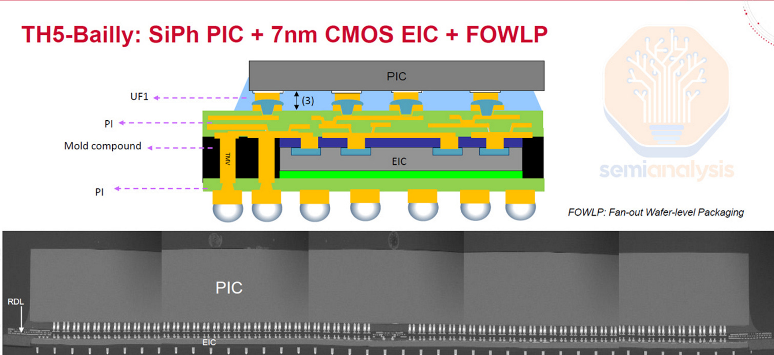
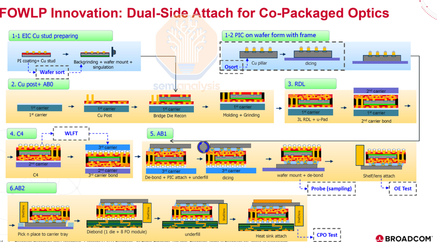
Broadcom reportedly transitioning from fan out wafer level packaging (FOWLP) with SPIL for is CPO solution to TSMC COUPE
FOWLP approach doesn’t allow scaling beyond 100G per lane due to excessive parasitic capacitance, as electrical signals must pass through the through mold vias (TMV) to get to the electric integrated circuit
Panel packaging
Have been working on panel packaging for over 6 years (2025)
Running pilot line for customer qualification for 600mm x 600mm late 2025/early 2026 (1Q25)
Testing
Largest provider of outsourced test services globally
Test services include
Wafer sort
Final test
System level test
Burn in
Currently primarily do wafer sort test. But have been investing to do final package test including burn in for late 2025/2026 (2Q25)
Can offer standalone test services, as well as combined full flow packaging and test service
Amkor
Known to be leader for automotive OSAT
Decades of experience meeting the stringent requirements of auto industry
E.g. Automotive certification (AEC-Q100) requires robust assembly
Have key facilities in EU and Japan
Manufacturing
Have fungibility of equipment between 2.5D advanced packaging types including
With silicon interposer
With RDL interposer
With silicon bridge embedded in interposer
Vietnam
Started production in 3Q24, ramping in 4Q24
Chosen for low cost structure
Mainly for consumer device market i.e. SiP
But also NAND and some 2.5D coming online (2Q25)
Migrated some SiP from Korea to Vietnam
To free capacity in Korea for advanced packaging
Act as second source alternative to China
5 of top 10 customers are qualifying Vietnam
Started with 2 lead customers
South Korea
Setting up to be able to do packaging and testing at the same place
Broke ground on new building in late 2025
Investing in tester fleet for high density digital pins and power supplies (2Q25)
Include burn in, SLT, and temperature stability handling systems
Phase 1 projected to be operational by end of 2025
Add 4000-6000 sq ft of test floor
Phase 2 est 1H27
Est to add another 40% capacity
Equipment moving in end of 2026
Bringing online 2.5D technology (2Q24)
Also have R&D facility
Japan
Mainly for auto and industrial packaging lines
Began to rationalize packaging lines (3Q25)
Due to underutilization in the auto market
Mainly in the mature side i.e. microcontrollers and traditional analog products
Note, did a similar rationalization in 2022
Closed 3 locations and reduced headcount
Working closely with customers on the taper down
Will raise prices for customers that remain to manage profitability
Will expect to finish taper down by 2027
Expect 100 bps improvement in company gross margin %
Portugal
In support of EU auto sector
Include advanced power modules such as SiC, GaN
Have partnership with Infineon
Arizona, US
Total $7b investment earmarked
Increased from $2b announced initially
Total 750k sq ft of clean room space
Most of capex will come in 2026 and 2027
Will be built in 2 phases
Phase 1
Broke ground in 3Q25
Est $2b investment
Expect to be completed mid 2027, with ramp in 2028
Est to be accretive to profitability 2 years after (i.e. 2030)
Est to contribute 10% of revenue
Phase 2
Announced phase 2 due to additional demand for US onshoring
Timing will be dependent on demand
Will be constructed with automation in mind
Will be located close to TSMC fab location
Will align TSMC technology nodes with Amkor packaging technology
However, not exclusive to TSMC
Amkor can also go direct to customers
CHIPS Act grant and investment tax credit would total approx $800m
Grant money will have a lag until it is received
Cost to be managed using
Level loading agreements
Guarantee stable, and consistent wafer volumes over time (e.g. X wafers/month or quarter)
Will help maintain high utilization
Low mix, high volume focus
Turnkey services
High automation
Also investing in testing facilities
Go to market
Have joined TSMC 3D Fabric Alliance (2022)
Signed agreement with TSMC to collaborate with TSMC on advanced packaging and testing in Arizona, US (2024)
Jointly define which packaging technologies to employ
Will effectively share end customers
Include some level of technology sharing
Likely to include Apple and Nvidia
Designed Process Assembly Design Kits (PADKs) and a design flow to achieve electronic design automation (EDA) connectivity with Cadence and Mentor Graphics
This is because designing chips need to have manufacturability and packaging in mind (i.e. design for manufacturability)
Packaging
Offer over 3000 different package formats and sizes
TSMC outsourcing
It is believed that Amkor also does a share of the wafer on substrate (WoS) portion of CoWoS
Split share with ASE Technology
Amkor will likely take 100% share of any TSMC CoWoS outsourcing at the Arizona, US fab
Completion scheduled for mid 2027
May also be outsourced the full flow for CoWoS
SiP (system in package)
Offers multi component, multi function products in an IC package
Embedded passive and active components
Offer double sided assembly
Chips attached on both sides of substrate
Include antenna in package (AiP) solutions
Amkor serves both iOS and Android market
Has been working with Apple for >10 years as SiP provider (for communications or RF)
Rumored to have lost mmWave AiP module for iPhone 15/16 generation (2024)
But then regained it back in 3Q25
SLIM (siliconless interconnect module)
2.5D
Amkor provides 2.5D packaging with silicon interposer with TSV
However note that Amkor does not manufacture the TSV themselves
Instead, they take wafers that have TSV already formed from foundry
“It is essential to distinguish that Amkor does NOT provide TSV formation in foundry wafers” ( https://amkor.com/technology/25d-3d-tsv/)
Amkor takes wafers in which ‘blind’ TSV have already been formed
It is ‘blind’ in the sense that the TSV stops partway through the silicon
I.e. you cannot see the TSV from the backside (until you thin the wafer)
Then thin wafer to expose TSV to complete the TSV interconnect structure
Wafer may start around 775um thick, then thinned down to 50-100um depending on the design
Then complete backside metallization to complete the connection to TSV
It is implied from earnings calls that Amkor provided packaging for Nvidia H20
Amkor notes that it has expanded customers from 2 to 4 (Nasdaq conference, Dec 25)
Increased revenue 4x from 2023 to 2024
Currently around single digit % of revenue (2Q24)
[Rumored to include Broadcom for networking and TPU in 2026/27]
[Also Nvidia GB10 for DGX Spark]
WLFO (wafer level fan out)
Licensed eWLB (embedded wafer level ball grid array) technology from Infineon
Similar to TSMC InFo and ASE FOCoS
Die is placed onto carrier, embedded in mold, and then RDL formed directly on top
Solder balls then attached to RDL, which is attached to substrate
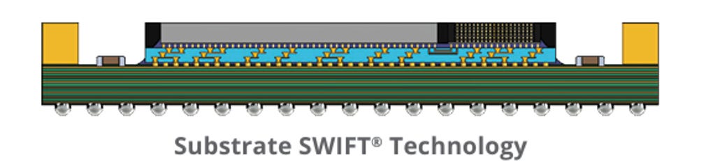
SWIFT (silicon wafer integrated fan out)
Amkor’s technology for high density fan out wafer level packaging
L/S of 2/2um
S-SWIFT (substrate-SWIFT or silicon wafer integrated fan out on substrate)
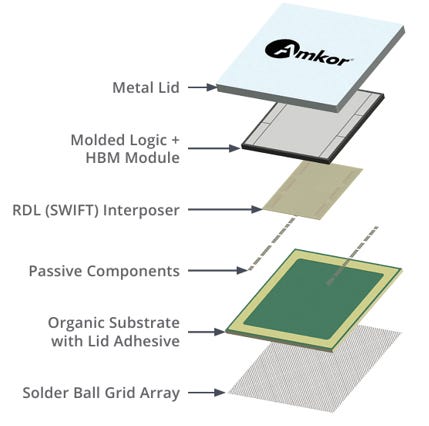
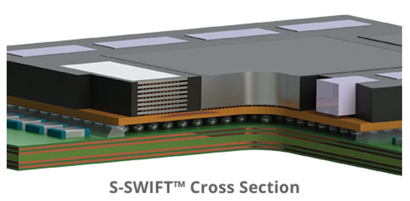
Equivalent to TSMC InFO-R
Flip chip chips onto RDL, then mounted on to BGA substrate
Supports >1,000 I/Os
2-6 RDL layers
Provide lower cost alternative to TSV 2.5D
Used for high I/O devices such as networking and server chips
Engaged between 5-10 customers (2Q24)
Launched with 1 existing customer and 3 new customers (1Q24)
First customer ramped (3Q25)
Second customer qualified and beginning ramp (Dec 25)
S Connect
Uses embedded silicon bridge embedded in fan out structure
Similar to Intel EMIB and TSMC CoWoS-L
Silicon bridge can either be connected using microbumps or TSV
TSV used for ASIC + HBM integration
Supports integrated passive devices (IPD) embedded in mold
Power delivery line from top die to substrate can be connected using through mold vias (TMV)
Utilizes RDL first/chip last process
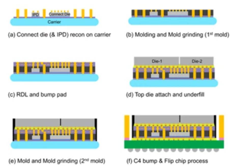
Silicon bridge die, IPD and copper pillars connected onto carrier wafer
Then encapsulated with mold and grinded to expose copper connections
RDL then fabricated on the mold
Top die attached to RDL with microbumps
Package then encapsulated again with mold
Carrier wafer then removed
C4 bump then added and attached to package substrate
Have 2 customers in qualification
Expected to ramp 2026 (1Q25)
Testing
>3600 testers in 8 locations
Additionally, have >600 cosigned
>10b units and >1.8m wafers tested annually
Operate 24/7 on fully networked test floors (i.e. software connected environment)
ATE, handlers, probers, data management tools are coordinated and centralized
Dynamic scheduling of test jobs across available ATEs
Test cell pooling across product families
I.e. multiple product types share the same pool of test equipment
Remote monitoring and control
Typically co located with packaging
Provides efficiency and avoid moving between countries
Can provide geographical diversification as most of global test capabilities is in Taiwan
Typically generate margins above corporate average
Known for RF test services
TSMC
TSMC has significantly gained share in advanced packaging, primarily due to integration of front end and back end processes for Apple and Nvidia
Apple is the key customer for InFO and Nvidia is the key customer for CoWoS
InFO (integrated fan out)
InFO-R (RDL interconnect)
Used for Mac M series chips (e.g. M1, M2, M3)
Typically 2-5 RDL layers
InFO-SoIS (system on integrated substrate)
Up to 14 RDL layers
However avoids using conventional ABF substrate stack up
Enable complex wiring between layers
InFO-SoW (system on wafer)
Allow fan out to the size of the entire wafer
E.g. Tesla Dojo 1
InFO-L (local silicon interconnect + RDL)
Include silicon bridge beneath the dies
Can be either passive (metal routing) or active (contain transistors)
First used in M1 Ultra to connect multiple M1 Max chips
Apple branded it ‘UltraFusion’ architecture
>10,000 signals between dies with 2.5TB/s of die to die bandwidth
Later also M2 Ultra
InFO PoP (package on package)
Can stack memory on top of processor
Used to reduce thickness and improve thermal efficiency
Used for Apple iPhones starting with A10 (iPhone 7)
Also Apple Watch S series
SPIL reportedly lost Apple’s A10 packaging to InFO in 2016
InFO oS (on substrate)
Designed for integrating multiple logic chiplets onto a substrate
Used for networking SoC, and HPC accelerators that want to avoid costly silicon interposer
InFO AiP (antenna in package)
Integrates the antenna directly into the chip package
Reducing size and improving signal gain and electrical performance
Used in 5G mmWave front end modules
InFO MS (memory on substrate)
Designed to integrate HBM with HPC logic dies
Wafer level multi chip module (WMCM)
Evolution from InFO
Unclear what the exact structure is
To be adopted for A20 chip used for iPhone 18 on 2nm process
Expected 3Q/4Q 2026
Will also use molding underfill (i.e. integrates the underfill and molding processes)
CoWoS (chip on wafer on substrate)
CoWoS-S (silicon interposer)
Interposer area has increased up to 3x reticle limit
Use of reticle stitching
Uses embedded deep trench capacitor (eDTC) integrated into the silicon interposer as a passive device
Deep trench structures etched into the silicon interposer
Filled with high density dielectric to form capacitors
Used to smooth voltage and maintain signal integrity
As chips operate at very high currents and high frequencies
Help deliver stable power and reduce voltage droop
New thermal interface material (TIM) for lid package
Server ODMs were overtightening the cooler screws
Caused the die to crack
So TSMC used a package that had a lid ‘over’ the die rather than directly on the die
Used for Nvidia Ampere A100 and Hopper H100
CoWoS-R (RDL interposer)
Silicon interposer replaced with organic RDL
Sacrifices some I/O density for cheaper cost
In RDL last/chip first approach, the RDL cannot be tested until it is already attached to the dies
This means that bad interposer can subsequently cause loss of good dies
Can be resolved using RDL first/chip last approach
TSMC can achieve L/S of 2μm/2μm
Minimum microbump pitch of 4um
Better electrical performance due to
The co-planar Ground-Signal-Ground-Signal-Ground (GSGSG)
Co planar refers to being on the same metal layer
GSGSG refers to ground trace in between two signal traces
Reduces capacitive and inductive coupling laterally, on the same layer
Capacitive coupling refers to when the electric field caused by the change in voltage in one line, pushes or pulls electrical charge on the nearby line
Inductive coupling refers to when a changing current in one conductor creates a changing magnetic field that induces a voltage in a nearby conductor
Also interlayer ground shielding with RDL interconnections
I.e. a ground plane is put between signal layers
Reduce Reduces capacitive and inductive coupling vertically, between layers
Help reduce cross talk, more stable impedance, fewer reflections, cleaner eye diagram, and lower electromagnetic interference (EMI)
The signal trace and its return path create a magnetic field around the loop
If you do not give the signal a nearby ground reference, the return current spreads out, the loop area gets bigger
With ground conductors right next to the signal, the return current has an easy low impedance path
Smaller loop area means lower inductance
CoWoS-L (local silicon interconnect + RDL)
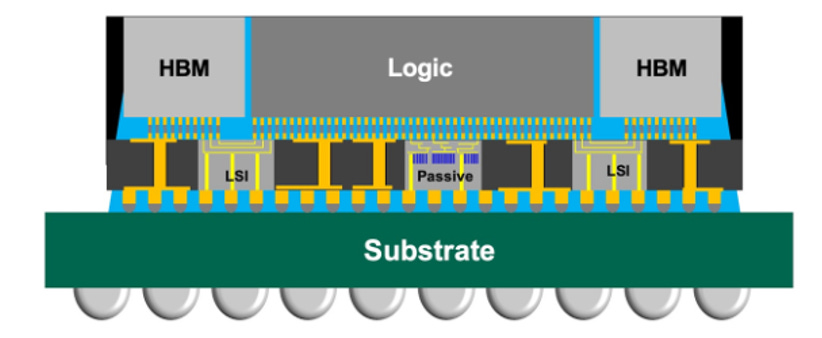
Contains an active or passive silicon bridge used for die to die interconnect
Embedded inside the interposer
Also embedded deep trench capacitor (eDTC)
Up to 6x reticle size limit
Used for Nvidia Blackwell (B100/B200/B300)
SoIC (system on integrated chips)
TSMC 3D packaging technology which includes both
Chip on wafer
Wafer on wafer
TSV interconnect pitch of <15um (v.s. 40-55um for microbump)
Customers include
Graphcore
AMD V cache
17um bond pitch
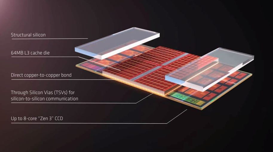
[Apple M5 Max/Ultra]
[AMD AI accelerators]
COUPE (compact universal photonic engine)
Codeveloped with Nvidia and Broadcom
Used for copackaged optics
Integrating electronic circuits with photonics circuits in a single package
Uses system on integrated circuit (SoIC) 3D stacking to connect electronics circuit and photonics circuit using copper to copper hybrid bonding
Intel
EMIB (embedded multi die interconnect)
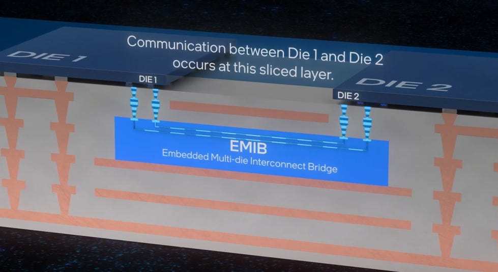
Uses small silicon die bridge embedded in ABF substrate
EMIB-T
T refers to the use of TSV
Original EMIB would require some signal and power routed through the interposer
Used in
Intel Sapphire Rapids
Rumors that Google TPU v8e variant will utilize intel EMIB-T packaging technology ( https://www.ctee.com.tw/news/20260102700057-430501)
Comes after NVDA has secured most of CoWoS supply
Aligns with reports that MediaTek was exploring intel EMIB-T after securing orders for v7e and v8e
MediaTek reportedly recruiting engineers experienced in intel EMIB technology
Other rumors of customers exploring EMIB include
AWS Trainium 4
Apple
Meta MTIA v4
Nvidia
Foveros
Foveros
36-50um bump pitch
Used in
Lakefield CPU
Ponte Vecchio GPU
Foveros Omni
‘Omni’ refers to omni directional interconnect or ODI
Serves as either
Active bridge between 2 dies underneath
Active die fully underneath another die
On top of another die but overhanging
~25um bump pitch
Used in
Meteor Lake
Arrow Lake

OD
Bumps
Compute/FXGA'M
Standard
Package Trace
Package Substfi
Package")
Foveros Direct
3D stacking using hybrid bonding
<10um bond pitch
Samsung
Advanced packaging technology branded as Advanced Packaging Fab Solutions (APFS)
However, has failed to gain significant traction with external customers
I-Cube
Silicon interposer 2.5D packaging technology
Similar to CoWoS-S
Supports 3x reticle size, and 8 HBM packages
X-Cube
3D stacking technology with hybrid bonding
Planned for 2026
4um bond pitch
King Yuan Electronics (KYEC) (TSE 2449)
Founded in 1987, based in Hsinchu, Taiwan
Largest pure play testing company
Second largest by revenue (after ASE)
Suitable for fabless design companies that use multiple OSAT houses that want to maintain IP privacy
Can also partner with any packaging vendor
OSAT providers may have testers tied up with their packaging lines
Not as easy to reconfigure for other customers/demand
Provides testing service, wafer grinding, dicing, and pick and place
Can provide the full flow of test from wafer sort, final test, burn in, SLT
ASE and Amkor have only just begun focusing more on final test, burn in and SLT
Have historically focused on wafer sort
Also has the scale to “get hundreds of testers up and running for you in weeks”
Over 4,300 test platforms in total
Tests 1.5 billion IC per month based on capacity
Gross margin and profitability are heavily dependent on utilization of testers
Also has inhouse division that can make custom test interface hardware
E.g. probe cards, load boards, contactors, (potentially modifying handlers), etc.
Can speed up ramp up time for a new product without having to wait for third party vendors
Manufacturing
Increased capex in 2025 to NT$37b, +40% y/y
Expedited the adoption of smart manufacturing practices
Key advantage is close proximity to TSMC and fabless firms in Taiwan
Taiwan
Floor area of 434,000m2 with cleanroom area of 207,000m2
2 main factories in Chunghwa and Tongluo
Aggressively expanding capacity in Taiwan for AI/HPC
Emergency new factory in Toufen (Miaoli) completed within months by end of 2024
Singapore
Invested approx SG$100m as means of exploring international expansion
US
Evaluating potential facility to serve key US clients locally
China
Divested its majority 92.1% stake in Suzhou King Long Technology, China based packaging/testing subsidiary for NT$21.7b (US$0.7b) in 2024
Due to geopolitical and competitive pressures
First invested in 2002 to serve customers in China
Freed up cash to be reinvested back into high end test capacity
Has regional offices in North America, Japan and Singapore to provide local sales and support
Go to market
>80% of customers are fabless design firms
IDM representing ~18%
Foundry representing ~2%
E.g. foundry may subcontract wafer sort to KYEC
For advanced testing needs, KYEC likely engages early during chip development to provide ‘design for testability’ (DFT)
I.e. design chip with how the device is going to be tested in mind
Locks in KYEC as vendor of choice
Also accelerates time to market
Has ‘test platform conversion’ offering where customers can move test program from one test platform to another e.g. Advantest to Teradyne
Provide extensive engineering support
Test program development
Debug
Yield improvement feedback
By providing one stop shop for all testing needs, smaller fabless company can effectively use KYEC dedicated account team as extension of their design team
Testing
Include full range of testing phases including
Wafer sort/wafer probe (~35% revenue, 2024)
Can test up to 128 sites in parallel
Bump pitch of 500um
Pogo pin probe card designed by KYEC
Final product test (~44% revenue, 2024)
System level test
Testing the chip in a scenario close to its end use environment
Catches defects that may have been missed by standard ATE test
Burn in
Operating chips at elevated temperature and voltages for extended periods of time
Screen out ‘infant mortality’ risk
Advanced process products accounted for 33% of 2024 revenue
AI/HPC testing made up 25% of KYEC revenue in 2024
The shift to advanced packaging (2.5D/3D, chiplets) and higher frequency devices demands new test methodologies and equipment
Less likely to see pricing pressure compared to mature products
Testers used for mature products more fungible relating to tester specifications, probe card customization, sockets, etc.
Testers for advanced products highly specialized and custom made for the exact device
KYEC have been investing in testers that can handle very high I/O (SerDes of tens of Gbps)
Also very large pattern memory to simulate real workloads
For pricing
High volume simpler devices might be priced per unit basis, e.g. $ per 1,000 units tested
For wafer sort, prices may be quoted on ‘per wafer’ or ‘per die’ sorted
Whereas complex devices might be effectively priced per hour due to long test times
If a device needs unique hardware (custom probe card, or socket) then KYEC might pass through those non recurring engineer costs to the customer as an upfront charge
Many test contracts have an initial tooling charge for designing and fabricating test fixtures
KYEC will price based on effective throughput, depreciation, labor and overhead, and profit margin
Customers that provide guaranteed volume will usually get discounted rates as it can guarantee certain margin
Conversely, sporadic or low volume jobs will likely carry a premium
Pricing may often be quoted in USD
Semiconductor industry often deals in USD
Powertech Technology Inc (PTI) (TSE 6239)
Founded in 1997 with memory testing. Then expanded into packaging in 2000
OSAT known to specialize in memory packaging and testing
Memory is approx 1/2 of total revenue (2025)
ASE and Amkor also does memory packaging, but is small portion of their revenue
Provide full turnkey services for memory manufacturing
I.e. customers can send wafers and receive fully tested packaged memory chips
Also positioning itself to be able to do HBM packaging
PTI has been investing in logic and advanced packaging for diversification
Notably fan out panel level packaging (FOPLP)
Plans to increase capex from NT$19b in 2025 to >NT$40b in 2026 due to increased demand for FOPLP
~3/4 would be used for FOPLP technology
Owns significant stake in Greatek which specializes in packaging for logic IC
Manufacturing
Taiwan
Located in Hsinchu
2018 broken ground on new FOPLP facility in Hsinchu Science Park, i.e. Plant 3C
More equipment added through 2021-22
2017, PTI partnered with Toshiba and Kingston Japan to form a joint venture TeraPower Technology in Taiwan
Focused on testing
2024 started construction of Fengshan plant in Kaohsiung City, Taiwan
Japan
Also has majority stake in Tera Probe (for testing)
Japanese memory testing venture with Elpida Memory (later acquired by Micron in 2013), Advantest, and Kingston Japan
First invested in 2005. Then acquired Micron’s 39.6% stake in 2017
2017 acquired Micron Akita, Micron’s memory assembly/test facility in Akita, Japan
Renamed to Powertech Technology Akita
2018 established Powertech Japan Ltd
For advanced packaging
Likely serves Kioxia/WD
Singapore
Acquired Nepes Singapore in 2014 (renaming it PTI Singapore)
China
Divested Xian plant to Micron in 2023
As part of Micron’s right to purchase after a 6 year service contract is fulfilled
After selling the plant to Micron in 2015
There will be 1 year transition period
Revenue reduction took effect in 3Q24
Sold 70% stake in Suzhou to Shenzhen Longsys Electronics in Jun 23
Originally acquired in 2009
Divested for US$132m
Go to market
Key customers likely include
SK Hynix
Micron
Acquired Elpida
Kioxia/Western Digital
Top 3 customers account for 55% of total revenue (2024)
#1 customer: 22%
#2 customer: 21%
#3 customer: 12%
Samsung does packaging and testing inhouse
Also likely to include Taiwanese memory players including Nanya, and Winbond
Rumored to have won MediaTek smartphone application processor business
PTI generates non recurring engineering (NRE) revenue for new development (2024)
Est NRE of US$10/mth from 2H26, and US$20/mth in 2027 for FOPLP
Packaging
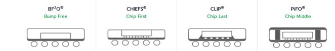
BF2O (bump free fan out)
No need for wafer bumping
For small I/O and few RDL layer count
Used in power management IC, power amplifier, audio
Min RDL L/S ≥15/15um
CHIEFS (chip first fan out)
Can do dual or triple die package
Min RDL L/S ≥5/5um
Used in application processor, baseband, ASIC, power management IC, memory
Cheaper than CLIP
CLIP (chip last fan out)
Utilize ‘known good RDL’ which avoids scrapping good dies
Include ability to embed passive components
Can do greater than triple die package
Used in CPU, GPU, FPGA
Thermal sensitive devices
Min RDL L/S ≥2/2um
PiFO (chip in middle fan out)
RDL layers both above and beneath die
Connected using copper pillars
Min. RDL L/S ≥5/5um on die backside, and ≥2/2um on die front side
Suitable for RF module, sensor, optical, 3D stacking, package on package
FOPLP (fan out panel level packaging)
Expected to enter volume production in 2027
Existing capacity has been fully booked by customers (3Q25)
Can only satisfy 50% of customers (3Q25)
Thus, increasing investment in 2026 to fulfil demand
Est for large rectangular panel to offer >3x throughput than existing 300mm wafers as a carrier
Instead uses 600mm x 600mm panels
3D IC
3D stacked packaged connected using microbumps and TSV
PTI making investment to be able to do TSV
Include CMOS image censor stacking
Used for automotive ADAS/autonomous systems
Via last process
IDM/foundry will do FEOL. Then send to PTI to do microbump, TSV formation, TSV fill, RDL (optional)
Via middle process
TSV and microbump are finished by MEOL process first by IDM/foundry
I.e. do interconnection step before die stacking
Then send to PTI to do singulation, thinning, die stacking using TCB
In 2023, PTI stated that they successfully developed HBM using TSV and high precision die stacking process
Potentially memory vendor can outsource HBM formation in the future
SiP
Differentiation in being able to integrate DRAM or NAND chips with logic in SiP
E.g. suitable for embedded multi chip package (eMCP) used in smartphones
I.e. combining DRAM and NAND with memory controller
Testing
Can be sold as a bundle with packaging, or standalone service
Can provide one stop shop from wafers, to fully tested final package
More common to do test along with packaging job, rather than standalone test
Does both wafer sort and final package test
Memory test important for speed binning DRAM
Also burn in test for DRAM and NAND reliability
Has decades of memory test expertise
Large library of memory test IP, i.e. pattern algorithms, diagnostic routes
Hana Micron (KRX 067310)
Founded in 2001
South Korea based OSAT provider
Full turnkey service provider including packaging and testing
Specializes in memory package and test
Also has subsidiary providing semiconductor materials, called Hana Materials
E.g. consumable silicon parts for etch equipment (silicon cathode rings)
The company proposed a split of the company into an investment holding company and operating company
But cancelled the spin off plan in Jul 2025
Shares increased 15% after the spin off plan was announced
Backlash from minority shareholders and legal disputes
Some said it was done for succession purposes (not uncommon in South Korea)
Manufacturing
Korea
Main production line
Brazil
HT Micron joint venture established in 2009 with Brazilian partner, Parit Participações
Also backed by Brazil government subsidies to support LATAM semiconductor needs
Vietnam
Established in 2016
Provide low cost production capacity
Proximity to Southeast Asia electronics customers
Go to market
Key customers include SK Hynix and Samsung
Potentially used as an a way to fulfil exceed demand during upcycles
Likely co develops packaging solutions with both companies
However, Hana Micron has also expanded to non memory customers
Including NXP Semiconductors and Microchip Technology
Products
Leadframe packages
I.e. standard SOP, QFN, etc.
Ball grid array laminate substrate
Refers to packaging DRAM chips or NAND flash onto substrate with solder balls
Used for mobile DRAM, eMMC (embedded multi media card), MCP, etc.
Pioneered world’s first 8 layer stacked SiP USB flash drive in 2009
Has expertise in ultra thin die stacking (i.e. thinning wafers down to 30-50um)
Suitable for smartphone and IoT devices
Flip chip
Refers to wafer bumping (putting microbumps onto dies) then mounting onto substrate
Provides wafer level bumping through Hana WLS (wafer level solutions)
Hana WLS was spun off and considered an affiliate entity
Also has capability to do RDL at wafer level
Thermal compression bonding
Work on fine pitch TCB (<20um pitch)
Targeting <6 seconds per chip
As part of government backed R&D project
HANAflex
Commercialized in 2014
Flexible semiconductor packaging technology (e.g. flexible SD card)
Can thin dies to <50um
Encapsulates in special stress relieved structure that can bend without breaking
Suitable for wearables, smart cards, medical devices, etc.
E.g. intra oral dental x ray that allowed to bend while in patient’s mouth
Testing
Includes end to end from wafer sort to final test
Also includes module test for assembled modules, i.e. microSD cards, USB drives, SSD, etc.